Hardware reference
Parts
| Role | Part | Notes |
|---|---|---|
| MCU | ESP32-S3 DevKitC-1 class | Dual Type-C N16R8 |
| Temp / humidity | SHT40 | I2C (spares on hand); power silk VCC / VIN / VN |
| Pressure | BMP390 | I2C (spares on hand); power silk VCC / VIN |
| Display | Estardyn 2.0″ ST7789 | 240×320, 8-pin SPI, BL on header |
| Storage | TF / microSD mini reader | 3V3 6-pin SPI breakout (Temu pack) — Phase 8 |
| Breadboard | Solderless 830 | Full-size; one or two (tie rail gaps if split) |
| Jumpers | DuPont | M–M for board↔board / board↔rail |
v1 uses one SHT40 + one BMP390. Confirm silk and I2C addresses in Phase 4 (typical: SHT40 0x44, BMP390 0x76/0x77). No lux sensor on the bench yet.
TFT silk — this Estardyn panel
Header, left→right: GND · VDD · SCK · SDA · RES · DC · CS · BL.
- Confirm 4-SPI (silk R3 + R5).
- Some packs print
SCLfor the clock — same net asSCK. - RES and RST are the same reset pin.
- Phase 2 ties BL → 3V3; the backlight needs no GPIO.
Breadboard
Nothing is "wired" yet — the board already has metal clips under the holes. This lab uses a full-size 830-point board.
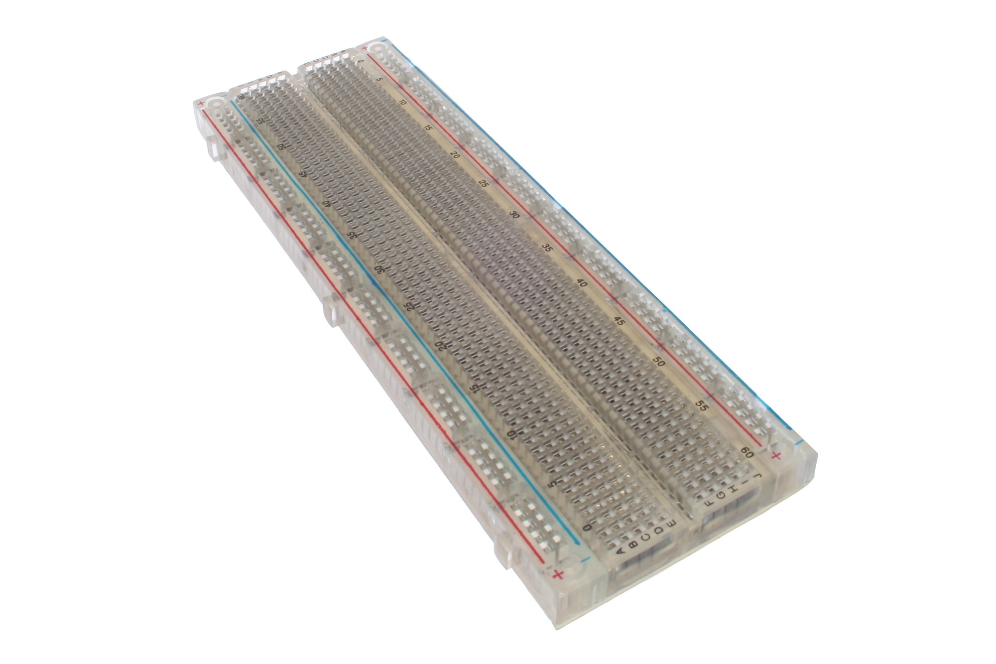
An empty 830 board — rows and rails are already tied as below.
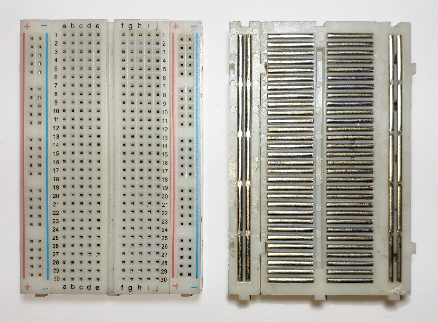
Top and underside: the same net rules apply across any 830 board.
| Region | How holes are tied (factory default) |
|---|---|
| Terminal strips | Each row of five (a–e or f–j) is one net. Same-number left and right are not joined. |
| Power rails | The + column is one vertical net; the − column is another. Red/+ → 3V3, blue/− → GND in this lab. |
| Rail gaps | Many boards break each rail halfway. Bridge with a short jumper if needed. |
Pick one + rail and one − rail as the 3V3/GND star. Run S3 3V3 and GND into those rails once, then tap modules from the rails.
Credit: empty 830 board oomlout / BREB-02 (CC BY-SA 2.0); connections diagram Guhuru (CC0).


One board or two
By Phase 9 this bench spilled onto a second breadboard — the top 830 holds the S3, display and sensors; a lower board carries the tact switch and status LEDs with room to spare.
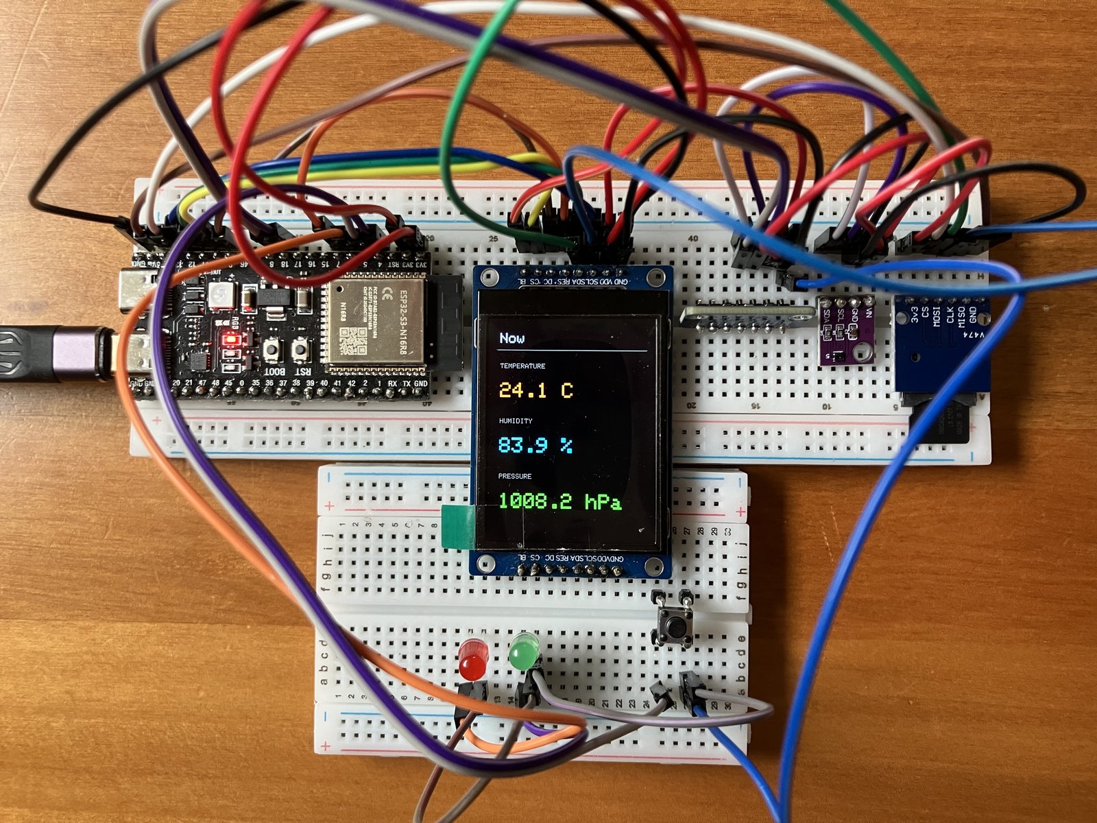
Two boards by Phase 9 — but a single 830 fits the whole build if you keep leads tidy. Tact cycles Now / Session / System.
The board count doesn't matter. What matters is that every net lands where the pin map says:
- One 3V3 rail and one GND rail shared across both boards — jumper rail-to-rail so the second board sees the same star.
- Each module's pin on the GPIO the pin map lists — verified by label, not by which board it sits on.
Split onto a second board only when the jumper nest gets hard to read.
Pin map
As-built through Phase 9. Match every connection by label.
ESP32-S3          SHT40          BMP390              ST7789
--------          -----          ------              ------
3V3        -----> VCC/VIN/VN --> VCC/VIN             VDD, (BL)
GND        -----> GND     -----> GND                 GND
GPIO8      -----> SDA     -----> SDI (I2C data)
GPIO18     -----> SCL     -----> SCK (I2C clock)
GPIO11     ---------------------------------------> SDA (MOSI)
GPIO12     ---------------------------------------> SCK (SPI clock; silk may say SCL)
GPIO10     ---------------------------------------> CS
GPIO9      ---------------------------------------> DC
GPIO7      ---------------------------------------> RES/RST
3V3        ---------------------------------------> BL (Phase 2)
3V3        ---------------------------------------> SD 3V3
GPIO13     ---------------------------------------> SD CS
GPIO11     ---------------------------------------> SD MOSI  (shared with TFT)
GPIO12     ---------------------------------------> SD CLK   (shared with TFT SCK)
GPIO14     ---------------------------------------> SD MISO
GND        ---------------------------------------> SD GND
GPIO5      ---------------------------------------> tact (other leg GND)
GPIO4      ---------------------------------------> green LED (+R) -> GND
GPIO6      ---------------------------------------> red LED (+R) -> GND
Sensors (I2C). BMP390: leave CS / SDO open for I2C; the data pin silk may say SDI or SDA.
microSD (Phase 8). This bench 6-pin silk: 3V3 CS MOSI CLK MISO GND (zeros may stand in for O). Share CLK/MOSI with the TFT; MISO = GPIO14, CS = GPIO13. Power from 3V3 only. Never share CS with the display (GPIO10).
Controls (Phase 9). Tact on GPIO5 (INPUT_PULLUP, other leg to GND). Green LED GPIO4, red LED GPIO6, each through a series resistor. No buzzer in v1.
Rules
- Modules are 3V3 — never feed 5V into sensor or TFT logic.
- Do not join TFT MOSI to I2C SDA.
- Avoid GPIO 0 / 19 / 20 / 38 / 48 / 45 / 46 (and 35–37 on Octal PSRAM).
- S3 underside silk is mirrored vs top — match by label.
Asset index
| File | What |
|---|---|
assets/breadboard-empty.jpg |
Empty full-size 830 breadboard |
assets/breadboard-connections.png |
Top + underside clips (same net rules on 830) |
assets/esp32s3-board-top.png |
S3 board photo |
assets/wiring-phase2-tft.svg |
Phase 2 TFT power (schematic) |
assets/wiring-phase3-sensors.svg |
Phase 3 SHT40 + BMP390 power (schematic) |
assets/wiring-phase4-i2c.svg |
Phase 4 I2C SDA/SCL (schematic) |
assets/wiring-phase6-tft.svg |
Phase 6 TFT SPI (schematic) |
assets/ui-phase7-climate.svg |
Phase 7 Climate UI mock (ST7789) |
assets/wiring-phase8-sd.svg |
Phase 8 microSD SPI (schematic) |
assets/wiring-phase9-controls.svg |
Phase 9 tact + status LEDs |
assets/bench-phase9-now.jpg |
Phase 9 — Now view |
assets/bench-phase9-session.jpg |
Phase 9 — Session (min/now/max) |
assets/bench-phase9-system.jpg |
Phase 9 — System (SD / sensors / append) |